At Intel‘s (NASDAQ:INTC) Technology and Manufacturing Day, hosted on March 28, the company disclosed a whole bunch of information about current and future manufacturing technologies. One of the more interesting disclosures the chipmaker made was the announcement of a new, low-cost technology that it calls 22FFL.
The technology, Intel says, is “the world’s first FinFET technology for low power [Internet of Things] and mobile products.”
Let’s take a closer look at the technology and the business rationale for why Intel is bothering to develop it in the first place.
A hybrid of 22-nanometer and 14-nanometer tech
In terms of physical dimensions and performance, 22FFL can be described as a “hybrid” of the company’s 14-nanometer tech and its 22-nanometer tech. As seen from the dimensions that Intel has provided for the technology, it’s closer in terms of chip area/density to the company’s older 22-nanometer tech than it is to the company’s current cutting edge 14-nanometer technology derivatives.
Image source: Intel.
From a performance and power perspective, however, 22FFL appears far better than the old 22-nanometer tech that Intel introduced back in early 2012.
Intel says 22FFL offers chip designers two transistor options: high-performance transistors and low-leakage transistors.
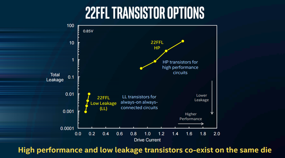
Image source: Intel.
As Intel explains, the high-performance transistors are suitable for use in portions of the chip that demand high performance (for example, CPU cores) and can deal with higher-leakage power, or what Intel calls “wasted power” in a glossary on its website, in exchange for higher performance. The low-leakage transistors, Intel says, are better fits for less performance-critical “always-on always connected circuits.”
The high-performance transistor options available in 22FFL, Intel claims, offers drive currents like what its state-of-the-art 14-nanometer++ technology does — at least in the range within which 22FFL can operate. As a chart that Intel provides shows, the performance of 22FFL’s high-performance transistors dramatically exceeds the high-performance transistors of its original 22-nanometer tech.
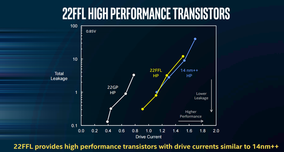
Image source: Intel.
The low-leakage transistor option, Intel says, “provides the lowest leakage transistors for any mainstream technology,” though the company didn’t offer hard data comparing its 22FFL with other commercially available technologies.
Both high-performance and low-leakage transistors, Intel says, can be used on the same chip design.
For both internal and external use
Intel is first and foremost an integrated design manufacturer, or IDM — which means the company both designs and manufactures its own chip designs. I suspect that 22FFL will be used extensively across Intel’s own product portfolio.
However, the company appears very interested in trying to get third-party chip vendors to use 22FFL as well.
Indeed, the company says the market for “leading-edge” foundry — that is, contract chip manufacturing — was around $23 billion in 2016. Intel defines “leading edge” as 28-nanometer technology or more advanced.
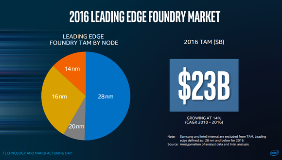
Image source: Intel.
Intel is courting mobile-applications processor makers as well as vendors of chips targeted at Internet of Things applications with 22FFL — not so coincidentally, the applications that require leading-edge technologies.
The company claims that 22FFL is “cost competitive with other 28/22 [nanometer] planar technologies,” supports a “wide range of advanced analog/RF devices,” and can deliver “die area scaling better than industry 28/22 [nanometer] technologies.”
The technology is expected to achieve “production readiness” in the fourth quarter of this year, meaning that we’ll start to see products using it in the marketplace in 2018.
At this point, it’s too soon to tell how much success Intel will have in getting third parties to use it, and frankly, it’s hard to even guess at how much success Intel might be able to find as a contract chip manufacturer. Intel has been advertising its foundry services for a while now, and it still hasn’t seen serious revenue flowing in from said services.
However, if Intel can manage to capture a reasonable amount of share here over the long term, then that could be an interesting potential growth vector for the company.
Ashraf Eassa owns shares of Intel. The Motley Fool recommends Intel. The Motley Fool has a disclosure policy.